ADC Buzzer Alarm - Tang Nano 9k
- Creating your Project
- Understanding the Project and the Blocks Used
- Connecting the Blocks
- Project Simulation
- Synthesis and FPGA Programming
- Hardware Validation
- Wrapping Up
Creating your Project
In this tutorial, you will learn how to configure a project that reads analog data from an ADC via the I2C protocol and, upon exceeding a predefined threshold, activates a buzzer. All development will be carried out in the ChipInventor platform, using preconfigured blocks for quick and efficient implementation.
Initial steps to create the project:
1. Open ChipInventor.
2. Click on New Project.
3. Fill in the following fields:
- Name: ADC Project with Buzzer
- Description: Analog signal reading with Comparison and Buzzer Activation
- Type: FPGA
4. Click Create to finalize the project creation.
Understanding the Project and the Blocks Used
The basic diagram of this project consists of reading data from an ADC (Analog-to-Digital Converter) via I2C. Then, based on the value read, we compare it to a threshold. If it exceeds that threshold, a buzzer sound is generated at a predefined frequency, with a periodic on/off pulse.
Below is an overview of the main blocks:
1. startAll
-
-
Releases system operation after a few clock cycles, generating the start signal.
-
Ensures that the other blocks only begin read/write operations after a short delay.
-
2. i2c
-
-
Implements the I2C protocol for communication with the ADC.
-
Contains input/output signals for sdaIn, sdaOutReg, and scl, as well as control signals (instruction, i2cEnable, etc.).
-
3. adc
-
-
Internally interfaces with the i2c block to configure and read the ADC value.
-
Sends commands to the ADC (via I2C) and receives the converted data, storing it in registers (e.g., Ch0, Ch1, etc.).
-
Typical output: 16-bit digital values representing the measured analog signal (e.g., Ch0, Ch1, Ch2, Ch3).
-
4. greater
-
-
Compares two 16-bit values, returning 1 if numa is greater than numb.
-
Here, we use it to check whether the ADC value exceeds a certain threshold (e.g., 10000).
-
5. two_hz_clock
-
-
Generates a 2 Hz signal (or a frequency defined by a parameter).
-
Used to pulse or “blink” a signal, in this case, creating an on/off effect for the buzzer periodically.
-
6. tune
-
-
Generates a waveform (square wave) at a desired frequency for the buzzer.
-
Receives the global clock and a frequency parameter (freq).
-
7. and3b, AND2b, inverterC
-
-
Logical blocks that assist in enabling or inhibiting combinational signals, controlling whether the buzzer is active at specific times.
-
Connecting the Blocks
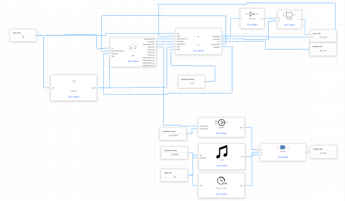
The diagram below illustrates how the blocks can be connected (this example follows the organization shown in the provided Verilog code).
1. adc (blk160_1)
-
-
Inputs:
-
clk: Connected to the FPGA’s main clock.
-
start: Received from the startAll block.
-
I2C outputs (e.g., complete, byteReceived).
-
-
Outputs:
-
Ch0, Ch1, etc., which represent the ADC’s channel readings.
-
Control signals (instruction, i2cEnable, byteToSend) that go to the i2c block.
-
-
2. i2c (blk159_4)
-
-
Inputs:
-
clk: Main clock.
-
sdaIn: Connected to the physical pin adc_sda (input mode).
-
Configuration signals for the ADC from the adc block.
-
-
Outputs:
-
sdaOutReg: Connected to the physical pin adc_sda (output mode, via tri-state logic).
-
adc_scl: I2C clock pin for the ADC.
-
complete, received: Status and data signals sent back to the adc block.
-
-
3. startAll (blk158_7)
-
-
Input:
-
clk: Main clock.
-
-
Output:
-
start: Goes low after a certain number of clock cycles, enabling the ADC read logic.
-
-
4. Comparison and Buzzer Activation
-
-
greater (blk19_29): Compares Ch0 to a fixed threshold (10000). If Ch0 > 10000, output is 1.
-
tune (blk202_25): Generates the waveform for the buzzer at a certain frequency (e.g., freq = 698).
-
two_hz_clock (blk107_33): Generates 2 Hz pulses, connected to the and3b block.
-
and3b (blk190_31): Combines three conditions (value > 10000, output from tune, and the 2 Hz pulse) to generate the final buzzer signal.
-
AND2b / inverterC: Internally control the SDA line and generate enable signals, following the project logic.
-
Finally, the buzzer pin (FPGA output) receives this final enable signal, causing an intermittent sound when the ADC value exceeds the defined threshold. At the end, it should be something like this:
Project Simulation
a) Steps to Simulate:
1. Access the Simulate Tab:
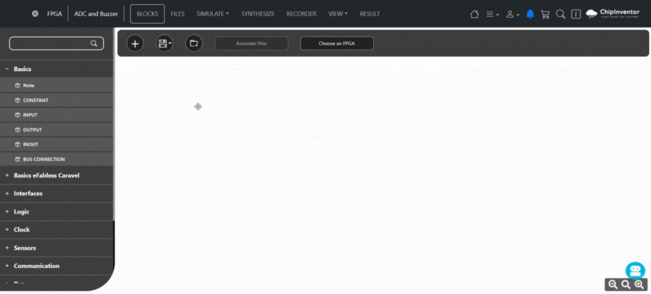
- Open the ChipInventor software and navigate to the Simulate tab in the top menu.
2. Select Advanced Simulation:
- Choose Advanced Simulation to get a detailed view of the simulation.
3. Start the Simulation:
- Click Run Iverilog (or a similar command) to compile and start the simulation.
b) What to Observe During Simulation:
✅ I2C Communication
-
Check whether the adc block initiates I2C communication after start is deactivated.
✅ Data Exchange
-
Confirm that data is being exchanged correctly between the adc and i2c blocks (e.g., byteReceived, i2cEnable, etc.).
✅ Channel Output (Ch0)
-
Observe whether Ch0 varies during simulation. (You can force simulated values for testing purposes.)
✅ Comparator Behavior
-
Verify that the greater comparator outputs 1 when Ch0 exceeds 10000.
✅ Buzzer Control
-
Check that the buzzer (final output) turns on and off based on signals from tune and two_hz_clock.
c) What to Do in Case of Errors:
If any issues arise:
-
Review the connections and configurations of the adc, i2c, and comparator blocks.
-
Verify the timing and signal types (e.g., bit widths).
-
Ensure the signals like byteReceived, i2cEnable, and other data exchanges are correctly implemented.
Synthesis and FPGA Programming
After verifying the simulation:
-
Click on the Synthesize tab.
-
Select Start Synthesis to generate the bitstream.
-
Wait until all items turn green, indicating a successful synthesis.
-
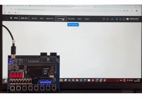
Connect your FPGA board to the computer via USB.
-
Select the correct serial port (often labeled “Enhanced” or similar).
-
Click Flashing to program the FPGA.