Implementation
The subprojects have led0 and led1 for visual confirmation of proper CAN communication, where both must be ON when working properly. In addition, both subprojects also use 4 pins of the FPGA to be connected at the CAN Transceiver: RX, TX, Vcc and GND. CAN PWM Duty Cycle Selector only uses the peripherals of the Devboard and 4 connections for the CAN Transceiver mentioned before.
Table 1 – System Specifications
|
Field |
Description |
|
FPGA Board |
Tang Primer 20K |
|
FPGA Core |
Gowin GW2AR-18 |
|
CAN Transceiver |
TJA1050 |
|
CAN Functionality |
Bitrate of 500 Kbps (See document at Links section) |
|
Input Interface |
- CAN PWM Duty Cycle Selector: 2 buttons for speed control and 1 for reset |
|
PWM Duty Cycle |
8-bit resolution (0-255) |
|
Clock Frequency |
27 MHz FPGA clock |
|
Power Supply |
5V via USB-A |
|
Programming Interface |
JTAG or USB Programmer |
|
PWM Duty Cycle Transmission Rate |
2 times per second (via CAN) |
|
Data Display |
Seven Segment Display for motor speed and duty cycle visualization |
|
Reset Functionality |
One reset button for each subproject |
Table 2 – System Connections
|
Component |
Connection/Terminal |
FPGA Pin or Power Supply |
|
CAN Transceiver TJA1050 |
VCC |
3.3V from FPGA |
|
GND |
GND from FPGA |
|
|
TX |
FPGA Pin D7 |
|
|
RX |
FPGA Pin D6 |
Block Diagrams
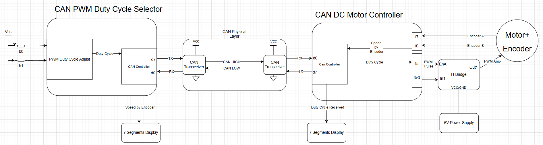
Figure 1 – Project developed at ChipInventor platform
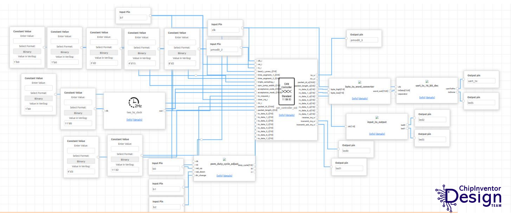
Figure 2 – CAN PWM Duty Cycle Selector subproject developed at ChipInventor