Creating and Using Testbenches
- Creating Flip-Flop Example
- Building Frequency Dividers
- Writing a Manual TestBench
- Explanation of Key Sections in the Code
- Running the Simulation
- Wrapping Up
Creating Flip-Flop Example
Welcome to our tutorial on TestBenches in ChipInventor. We’ll create a simple Flip-Flop circuit to highlight how to set up and run TestBench simulations. Rather than focusing on circuit details, this guide emphasizes verifying behavior and generating waveforms with the TestBench. By the end, you’ll know how to efficiently validate digital logic in ChipInventor and be ready for more complex projects.
a. Creating the Flip-Flop Project
1. Click New Project in the top menu.
2. Fill the project details:
-
Name: FlipFlop TestBench,
-
Description: Basic example of how to use testBench in ChipInventor.
-
Type: OpenRoad.
3. Click on Create Chip to start the project.
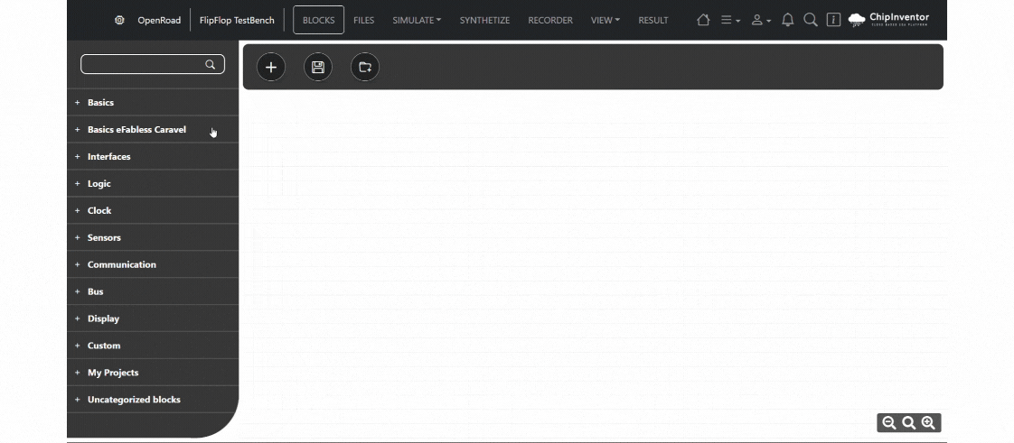
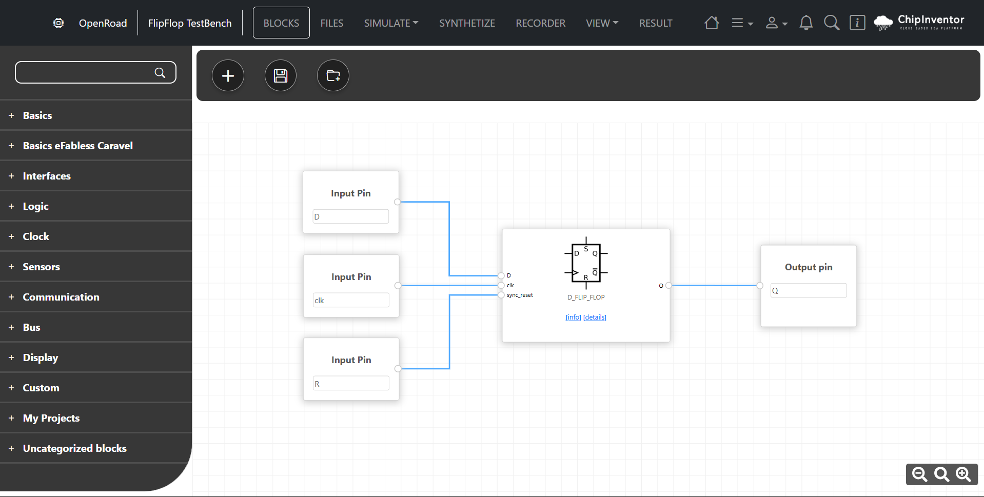
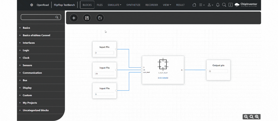
b. Flip-Flop in the Blocks Tab
1. Adding and Configuring the Flip-Flop
2. In the Blocks tab, locate the Flip-Flop D block and drag it to the workspace.
3. Add three inputs (Inputs) named:
-
Clock, D, and Reset (names can be customized to facilitate your understanding later).
4. Add one output (Output) and name it Q.
5. Connect the Clock, D, and Reset input pins to the respective Flip-Flop inputs.
6. Connect the Q output pin to the output block.
c. Configuring the TestBench
2. Select Advanced Simulation.
4. Click on Create VCD to generate a file that enables the visualization of circuit signals.
5. Use the integrated viewer to inspect the Clock, D, Reset, and Q signals.
6. In the bottom-right corner of the VCD page, click on the question mark icon to view shortcuts that can help improve waveform visualization.
d. Improving the TestBench
1. Editing Input Values
-
Locate the Verilog code in the left tab.
-
Adjust the input signals (for example, changing them from 0 to 1) to test different scenarios.
2. Re-running the Simulation
3. Understanding the Static TestBench
-
The default TestBench includes predefined sequences.
-
By manually editing the inputs, you create customized tests to better evaluate the circuit.
If you notice differences in the signals displayed in the newly generated VCD, it means your changes to the TestBench were successfully applied.
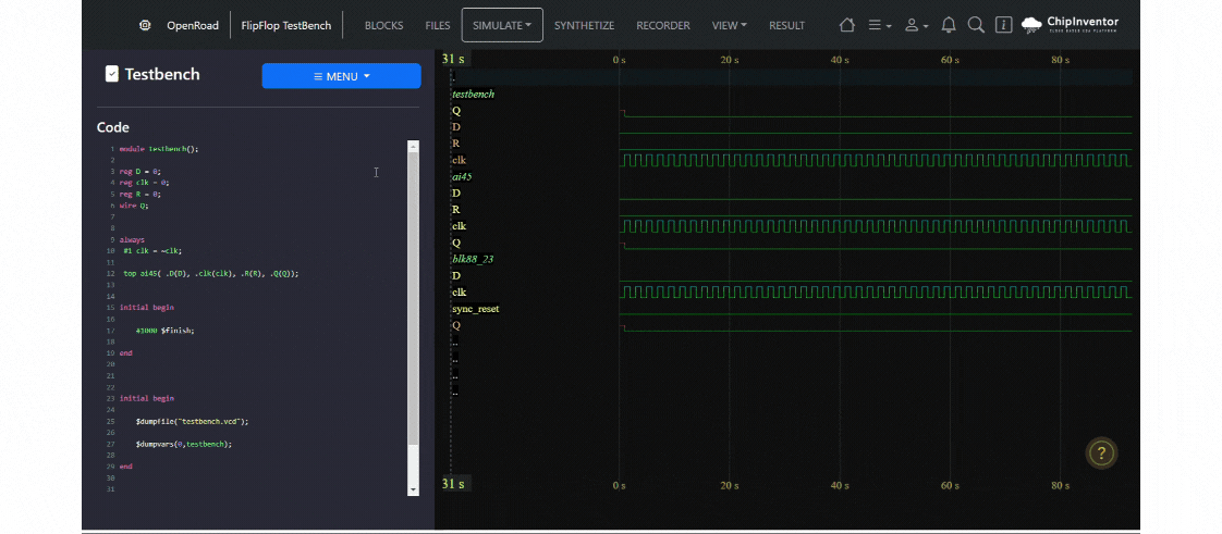
e. Analyzing the Results
-
Examine the waveforms generated in the viewer.
-
Ensure that the Q output responds correctly to the Clock signal and the Reset command.
-
Ask yourself: Does the Q output behavior match expectations regarding the clock and reset?
Building Frequency Dividers
In this section, instead of using an external clock signal, we will manually generate input transitions and define a custom TestBench to verify the behavior of the circuit. The goal is to demonstrate how to create a manual TestBench in Verilog instead of relying on the automated tools provided by ChipInventor.
1. Create a new project.
- Name: Manual TestBench - Frequency Divider
- Description: Manually verifying a frequency divider using a custom TestBench.
- Type: OpenRoad
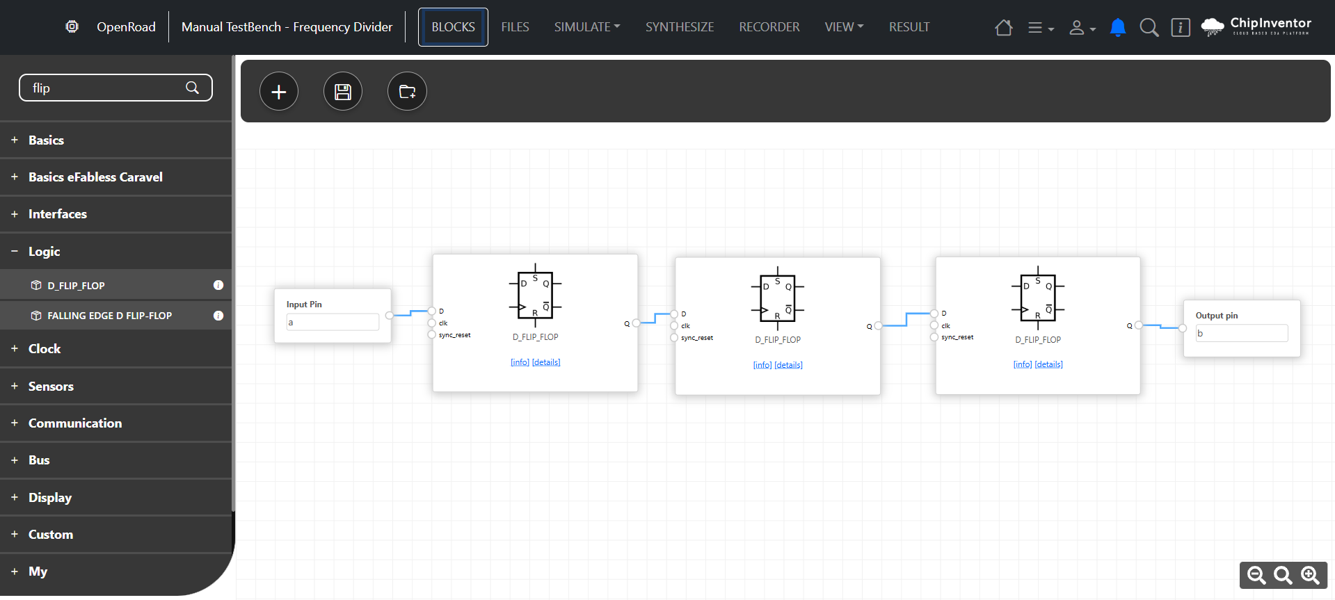
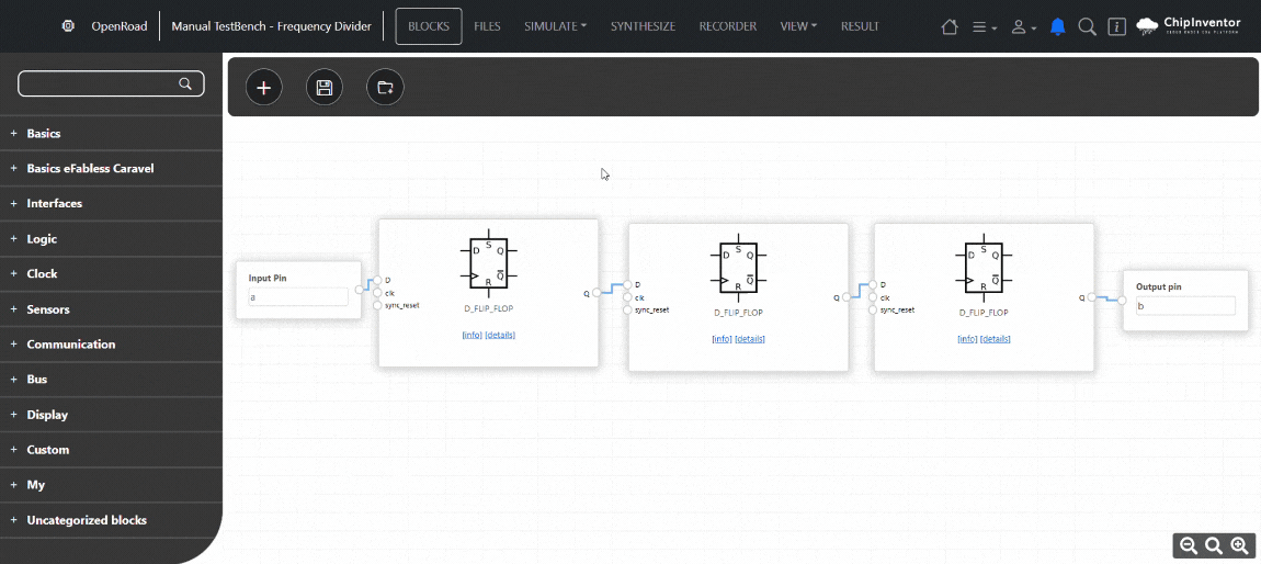
2. Insert multiple Flip-Flop D blocks into the workspace.
- The first Flip-Flop will store the initial state.
- Each additional Flip-Flop will take the previous one’s output as its own clock signal.
3. Connect the Flip-Flops in cascade.
- The Q output of each Flip-Flop should be connected to the D input of the next Flip-Flop.
- No external clock will be used; instead, we will control the D and Reset inputs manually in our TestBench.
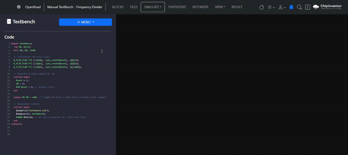
Writing a Manual TestBench
Since we are not using the automated ChipInventor TestBench, we need to manually define input signals in Verilog to simulate our circuit.
Steps to Write the TestBench:
-
Open the Verilog code editor in the Advanced Simulation tab.
-
Replace the automatically generated code with the following manual TestBench
module testbench;
reg b0, Reset;
wire Q1, Q2, led0;
// Instantiate the Flip-Flops
D_FLIP_FLOP FF1 (.D(b0), .sync_reset(Reset), .Q(Q1));
D_FLIP_FLOP FF2 (.D(Q1), .sync_reset(Reset), .Q(Q2));
D_FLIP_FLOP FF3 (.D(Q2), .sync_reset(Reset), .Q(led0));
// Generate a clock signal for b0
initial begin
Reset = 1;
b0 = 0;
#10 Reset = 0; // Release reset
end
always #5 b0 = ~b0; // Toggle b0 every 5 time units (creates clock signal)
// Simulation control
initial begin
$dumpfile("testbench.vcd");
$dumpvars(0, testbench);
#1000 $finish; // Run the simulation for sufficient time
end
endmodule
Explanation of Key Sections in the Code
To ensure that the reader can understand and modify the TestBench if needed, let's go through the main parts of the code:
1. Instantiating Flip-Flops
D_FLIP_FLOP FF1 (.D(b0), .sync_reset(Reset), .Q(Q1));
D_FLIP_FLOP FF2 (.D(Q1), .sync_reset(Reset), .Q(Q2));
D_FLIP_FLOP FF3 (.D(Q2), .sync_reset(Reset), .Q(led0));
-
Three Flip-Flops are instantiated and connected in cascade.
-
The first Flip-Flop receives the input signal b0, and each subsequent Flip-Flop takes the Q output of the previous one as input.
-
The last output (led0) represents the divided frequency after three Flip-Flop stages.
2. Clock Signal Generation
always #5 b0 = ~b0; // Toggle b0 every 5 time units (creates clock signal)
-
This command toggles b0 every 5 time units, effectively simulating a 10-time unit period clock.
-
As a result, b0 acts as a square wave signal.
3. Reset Initialization
initial begin
Reset = 1;
b0 = 0;
#10 Reset = 0; // Release reset
end
-
The Reset signal is initially set to 1 to clear all Flip-Flop outputs.
-
After 10 time units, Reset is set to 0, allowing normal operation of the Flip-Flops.
4. Simulation Control
initial begin
$dumpfile("testbench.vcd");
$dumpvars(0, testbench);
#1000 $finish; // Run the simulation for sufficient time
end
-
The $dumpfile("testbench.vcd") command stores all simulation data in a .vcd file for waveform analysis.
-
The simulation runs for 1000 time units, ensuring enough time to observe multiple frequency divisions.
Running the Simulation
To test the frequency division, follow these steps:
1. Run the TestBench in ChipInventor:
2. Generate the waveform file:
- Click on Create VCD to create the .vcd file with signal transitions.
3. Open the waveform viewer:
- Inspect b0, Q1, Q2, and led0 to observe how each Flip-Flop divides the input signal frequency.
Wrapping Up
This tutorial provided a practical guide for creating and validating Flip-Flops using ChipInventor. Through the practices described, you:
-
Configured and tested individual and cascaded Flip-Flops.
-
Used the TestBench to verify the expected behavior of circuits.
These fundamental concepts will serve as a foundation for more advanced projects, enabling the development of robust and effective digital solutions.