I2C Protocol
- Introduction to the I2C Protocol
- Creating the Project in ChipInventor
- Understanding the Project Blocks
- Assembling the Blocks in ChipInventor
- Project Simulation
- FPGA Synthesis and Programming
- Hardware Validation
- Wrapping Up
Introduction to the I2C Protocol
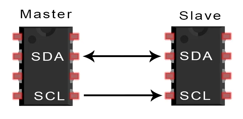
The I2C (Inter-Integrated Circuit) protocol is one of the most used communication protocols in embedded systems. It allows communication between multiple devices using only two lines:
-
SDA (Serial Data) → Bidirectional data line.
-
SCL (Serial Clock) → Clock line that synchronizes communication.
Each device connected to the I2C bus has a unique address. Communication always happens between a Master device (controller) and one or more Slaves (peripherals).
Basic Operation:
-
The Master starts communication by sending a START signal.
-
The Master sends the Slave address + read/write bit.
-
The Slave acknowledges the address by sending an ACK (acknowledge).
-
The Master transmits or receives the data.
-
The communication ends with a STOP signal.
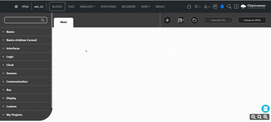
Creating the Project in ChipInventor
In this tutorial, we will create a project that uses the I2C protocol to read data from an ADC (Analog-to-Digital Converter).
Initial Steps:
1. Access the ChipInventor website.
2. Click on New Project.
3. Fill in the information:
- Name: I2C Communication with ADC
- Description: Data reading project using I2C protocol with an external ADC.
- Type: FPGA
4. Click Create.
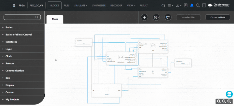
Understanding the Project Blocks
The main blocks used in this project are:
|
Block |
Function |
|
startAll |
Generates the initial signal for the system to start operating. |
|
i2c |
Controls the I2C communication, performing read and write operations. |
|
adc |
Controls the communication steps with the ADC via I2C. |
|
adcController |
Controls the data reading flow and stores the results. |
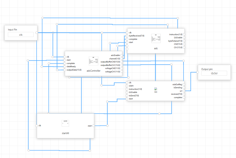
Assembling the Blocks in ChipInventor
Below are the connections that must be made between the blocks:
Block: startAll
- Input:
- clk → System clock.
- Output:
- start → Start signal.
- start → Start signal.
Block: i2c
- Inputs:
- clk → System clock.
- start → Output from startAll block.
- instruction → Operation instruction (write, read, start, or stop).
- i2cEnable → Enable I2C operation.
- byteToSend → Byte to send.
- Outputs:
- scl → I2C clock pin.
- complete → Indicates operation completion.
- byteReceived → Received byte from communication.
Block: adc
- Inputs:
- clk → System clock.
- start → Output from startAll.
- complete → Output from i2c.
- byteReceived → Output from i2c.
- Outputs:
- instruction → Input to i2c.
- i2cEnable → Input to i2c.
- byteToSend → Input to i2c.
- dataReady → Indicates that data has been captured.
- outputData → Data read from the ADC.
- adcEnable, channel → Inputs to adcController.
Block: adcController
- Inputs:
- clk → System clock.
- start → Output from startAll.
- complete → Output from i2c.
- dataReady → Output from adc.
- outputData → Output from adc.
- Outputs:
- adcEnable, channel → Inputs to adc.
- outputBufferCh0 and outputBufferCh1 → Stored data.
- voltageCh0 and voltageCh1 → Converted voltage values.
Project Simulation
-
Access the Simulate tab.
-
Click Advanced Simulation.
-
Click Menu → Run Iverilog.
-
Check for errors.
-
If necessary, correct the blocks and connections.
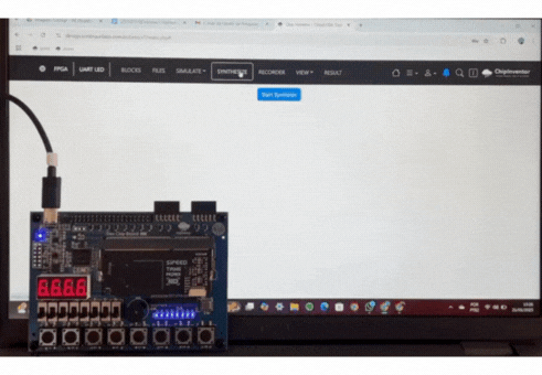
FPGA Synthesis and Programming
-
Access the Synthesis tab.
-
Click Start Synthesis.
-
If all items turn green, connect your FPGA to the PC.
-
Select the correct port.
-
Click Flashing to program the project.