SPI Protocol
- SPI Protocol Overview
- Creating the Project in ChipInventor
- Blocks Used
- Top-Level Connections
- Simulation
- FPGA Synthesis and Programming
- Hardware Validation
- Wrapping Up
SPI Protocol Overview
SPI (Serial Peripheral Interface) is a synchronous, full-duplex communication protocol used for high-speed data exchange over short distances. It follows a master–slave architecture with four primary signals:
-
SCLK (Serial Clock): Clock signal generated by the master to synchronize data transfers.
-
MOSI (Master Out Slave In): Data line from master to slave.
-
MISO (Master In Slave Out): Data line from slave to master.
-
CS_n (Chip Select, active-low): Signal used by the master to select the slave device.
Bits are shifted out on MOSI and shifted in on MISO on each clock edge, according to the configured clock polarity (CPOL) and phase (CPHA).

Creating the Project in ChipInventor
1. Open ChipInventor.
2. Click New Project.
3. Fill in the fields:
- Name: SPI Communication Tutorial
- Description: SPI Master–Slave Data Transfer with LED Display
- Type: FPGA
4. Click Create.
Blocks Used
|
Block |
Function |
|
spi_master |
Generates SCLK, MOSI, and CS_n; sends incremental byte values |
|
spi_slave |
Samples MOSI on SCLK rising edge; outputs data_valid pulse |
|
data_register |
Synchronously latches input d into q when load = 1 |
|
LEDs |
Displays the 8-bit output from the register |
Slave Blocks: On one workstation, instantiate and configure the spi_slave and data_register blocks. Record a GIF showing:

Master Block: On a separate workstation, instantiate and configure the spi_master block. Record a GIF that demonstrates:

Top-Level Connections
In this project, the FPGA Master and FPGA Slave are interconnected as follows:
-
Common signals (both FPGAs):
-
clk: system clock
-
rst_n: active-low reset
-
Master → Slave connections:
-
sclk: serial clock
-
mosi: master data output
-
cs_n: chip select (active-low)

-
Slave internal connections:
-
data_valid → load input of data_register
-
data_out[7:0] → d input of data_register
-
Final output:
-
data_register.q[7:0] → LEDs on the board

Simulation
1. Go to the Simulate tab and select Advanced Simulation.
2. Run Iverilog.
3. Check the console for compilation errors.
4. In the waveform viewer, monitor key signals:
- spi_master.byte_counter
- spi_slave.shift_reg
- data_valid
- data_out
5. Confirm that on each deassertion of CS_n, eight bits are received, data_valid pulses, and data_out matches the transmitted byte.
FPGA Synthesis and Programming
1. Open the Synthesize tab and click Start Synthesis.
2. Wait until all synthesis items turn green.
3. Connect your FPGA board via USB.
4. Select the appropriate programming port.
5. Click Flashing to program the master and slave bitstreams.

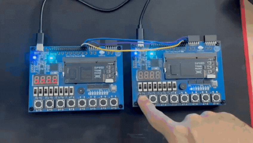
Hardware Validation
1. Power on both FPGAs.
2. Observe the slave’s LEDs—they should display the incrementing byte sent by the master.
3. If the LEDs do not update correctly:
- Verify the polarity and wiring of rst_n.
- Check connections for sclk, mosi, and cs_n between the boards.
- Adjust the CLK_DIV parameter in spi_master for proper timing.
4. (Optional) Use a logic analyzer to probe the SPI lines and verify signal integrity.
Wrapping Up
Congratulations! You have developed a complete SPI communication project using the ChipInventor platform.
Now that you understand the SPI protocol, you can expand this knowledge and implement communication with other sensors and devices.