Implementation
The subprojects have led0 and led1 for visual confirmation of proper CAN communication, where both must be ON when working properly. In addition, both subprojects also use 4 pins of the FPGA to be connected at the CAN Transceiver: RX, TX, Vcc and GND. The CAN Transceivers are connected together using their High and Low pins. For the CAN DC Motor Controller subproject, the generated PWM Signal are showed at led2 and is connected to the Enable channel of the H-Bridge module and his In1 input to the 3v3 of the FPGA, fixing the direction of the DC Motor to only one direction. The correspondent output of the H-Bridge module is then connected to the positive and negative DC Motor terminals. The phases A and B, 3v3 and GND of the built-in DC Motor encoder are then connected to the FPGA, finishing the connections of this subproject.The following table resumes all connections.
Table 1 – System Specifications
|
Field |
Description |
|
FPGA Board |
Tang Primer 20K |
|
FPGA Core |
Gowin GW2AR-18 |
|
CAN Transceiver |
TJA1050 |
|
CAN Functionality |
Bitrate of 500 Kbps (See document at Links section) |
|
Input Interface |
- CAN DC Motor Controller: 1 button for reset |
|
DC Motor Used |
GM-25 370 DC Motor with encoder(No load 6V 210 RPM) |
|
DC Motor Power Supply Used |
AC to DC 6V 2A |
|
H-Bridge Motor Driver Used |
L298n |
|
PWM Frequency |
15 kHz |
|
PWM Duty Cycle |
8-bit resolution (0-255) |
|
Speed Measurement |
Encoder pulses from PhaseA and PhaseB |
|
Clock Frequency |
27 MHz FPGA clock |
|
Power Supply |
5V via USB-A |
|
Programming Interface |
JTAG or USB Programmer |
|
Speed Transmission Rate |
20 times per second (via CAN) |
|
PWM Duty Cycle Transmission Rate |
2 times per second (via CAN) |
|
Data Display |
Seven Segment Display for motor speed and duty cycle visualization |
|
Sampling Frequency |
10 Hz (for motor speed measurement) |
|
Reset Functionality |
One reset button for each subproject |
Table 2 – System Connections
|
Component |
Connection/Terminal |
FPGA Pin or Power Supply |
|
L298N (Motor Driver) |
Vcc and GND |
6V 2A Power Supply |
|
Logic Level |
5V from FPGA |
|
|
ln1 |
3.3V from FPGA |
|
|
In2 |
GND from FPGA |
|
|
Motor + (Out 1) |
Motor connection (Motor +) |
|
|
Motor - (Out 2) |
Motor connection (Motor -) |
|
|
Enable 1 |
FPGA Pin F4 |
|
|
Motor Encoder |
Phase A |
FPGA Pin F7 |
|
Phase B |
FPGA Pin F6 |
|
|
CAN Transceiver TJA1050 |
VCC |
3.3V from FPGA |
|
GND |
GND from FPGA |
|
|
TX |
FPGA Pin D7 |
|
|
RX |
FPGA Pin D6 |
Block Diagrams
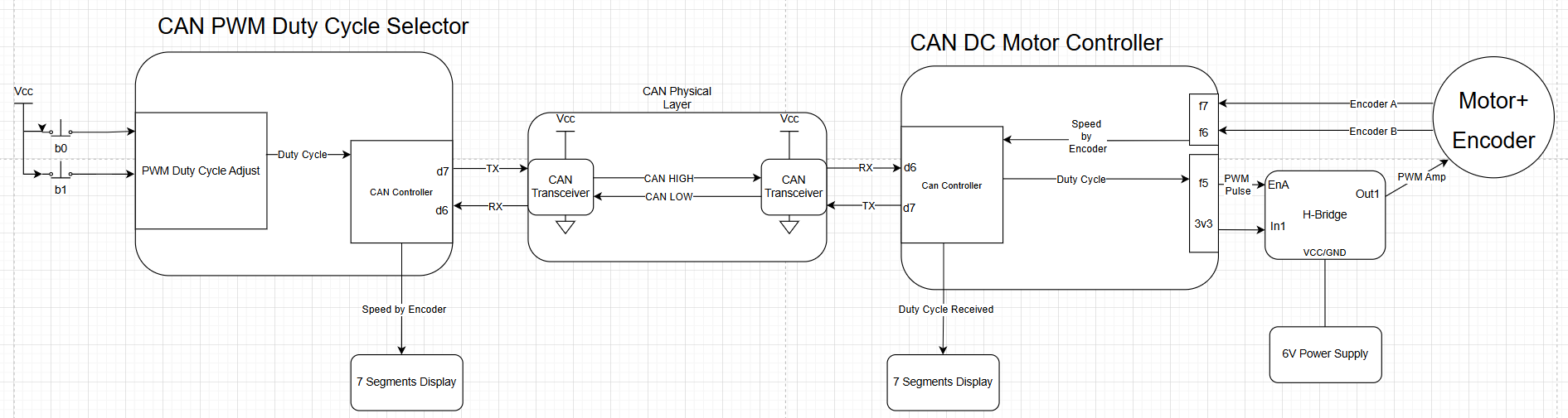
Figure 1 – Project developed at ChipInventor platform
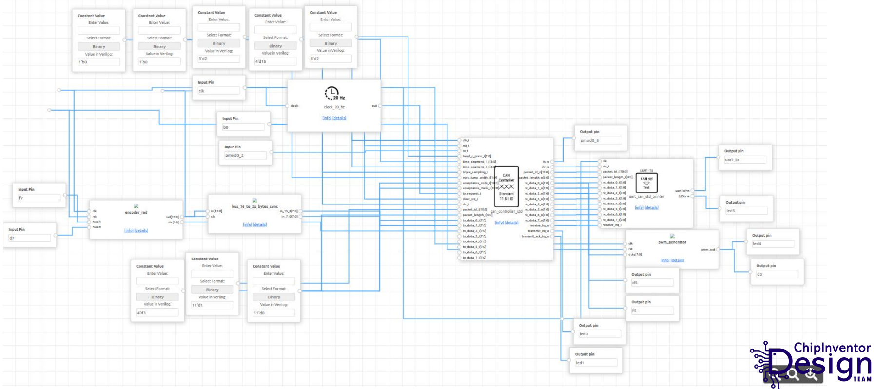
Figure 2 – CAN DC Motor Controller subproject developed at ChipInventor
No Comments