How to Use the INOUT Block in ChipInventor
1. Introduction
The INOUT block in ChipInventor allows you to configure an FPGA pin to operate bidirectionally, meaning it can function as either an input or output depending on the control signal. This feature is essential in various applications, especially in communication with external devices.
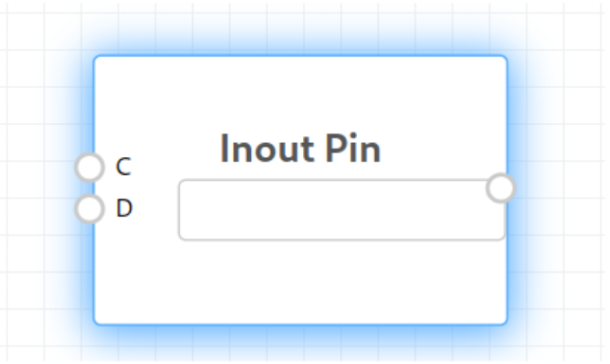
2. Structure of the INOUT Block
The block has three main parts:
-
Input D: Defines whether the pin operates as input or output.
-
D = 1 → Pin configured as OUTPUT.
-
D = 0 → Pin configured as INPUT.
-
Input C: Defines the output value when the pin is in OUTPUT mode (D = 1).
-
Output: Represents the value read from the pin when it is in INPUT mode (D = 0).
3. Code Generated by ChipInventor
When using the INOUT block, ChipInventor automatically generates the following Verilog code:
assign inout_pin = d ? c : 1'bZ;This means:
-
If d = 1, the pin takes the value of c (OUTPUT mode).
-
If d = 0, the pin goes to high impedance (Z), allowing another device to control it (INPUT mode).
The block also generates the connection in the module where the pin will be used:
module_x blk_example (
    .input_pin(inout_pin)
);
No Comments