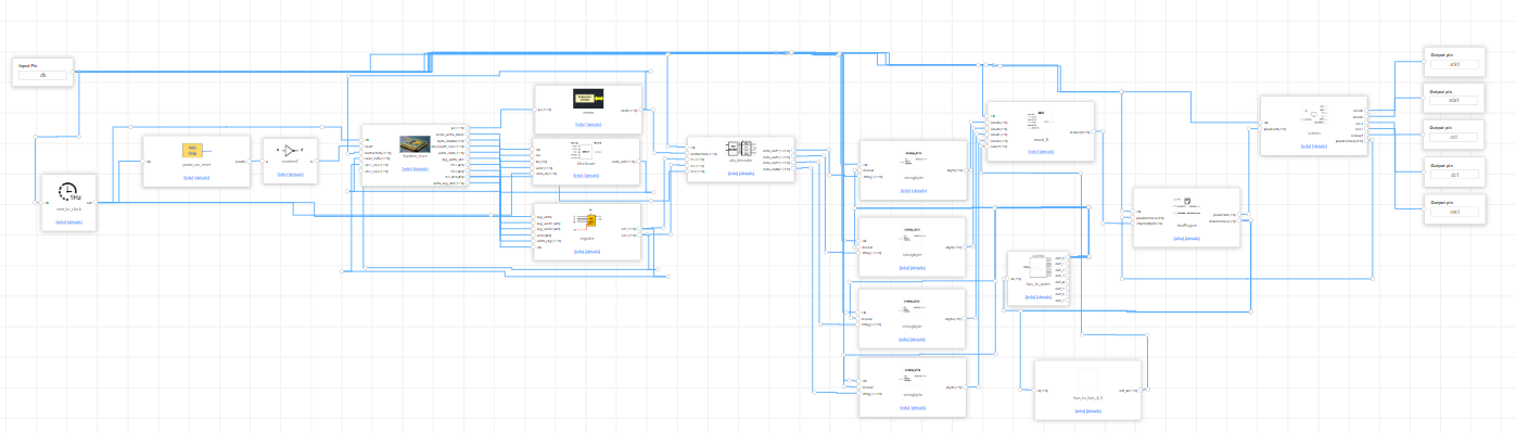
Connecting the Blocks
To assemble your project in the ChipInventor block diagram:
1. Drag each block (e.g., franken_riscv, imem, blockram, register) onto the workspace.
2. Connect the signals according to the Verilog code or as described in previous tutorials. Examples:
- The clk signal (from one_hz_clock or an Input Pin) should go to the clk input of franken_riscv, register, blockram, and other modules.
- reset (from inverterC or another reset block) connects to the reset inputs of these modules.
- The pc output of franken_riscv is fed into imem, which returns instr back to franken_riscv via instruction.
- For data memory, alu_result_Exec serves as the address (addr), write_data is the write input, and read_data is the output from blockram.
- RS1, RS2, RD, reg_write_WB, and write_reg_WB connect the franken_riscv to the register module.
3. If you plan to use a display, connect screen and textEngine as indicated.
4. Save your diagram and ensure all modules have correct clock, reset, and signals.
No Comments