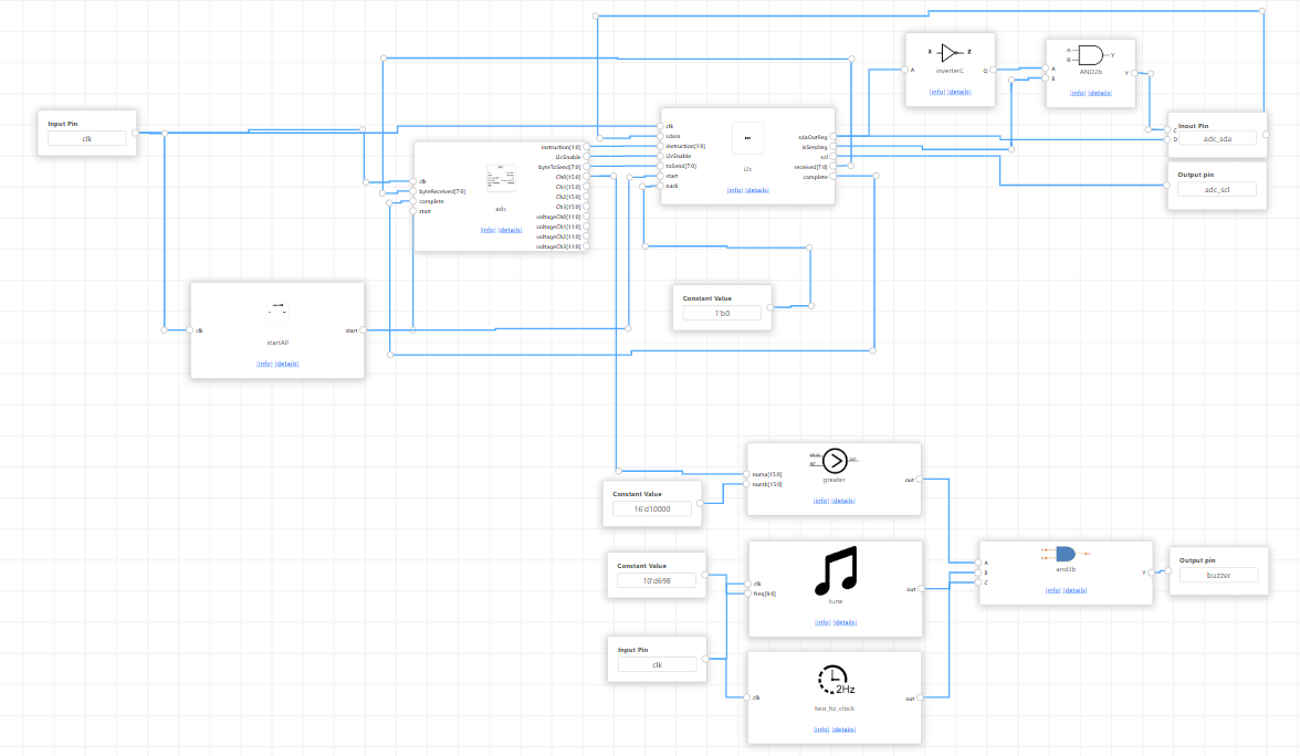
Connecting the Blocks
The diagram below illustrates how the blocks can be connected (this example follows the organization shown in the provided Verilog code).
1. adc (blk160_1)
-
-
Inputs:
-
clk: Connected to the FPGA’s main clock.
-
start: Received from the startAll block.
-
I2C outputs (e.g., complete, byteReceived).
-
-
Outputs:
-
Ch0, Ch1, etc., which represent the ADC’s channel readings.
-
Control signals (instruction, i2cEnable, byteToSend) that go to the i2c block.
-
-
2. i2c (blk159_4)
-
-
Inputs:
-
clk: Main clock.
-
sdaIn: Connected to the physical pin adc_sda (input mode).
-
Configuration signals for the ADC from the adc block.
-
-
Outputs:
-
sdaOutReg: Connected to the physical pin adc_sda (output mode, via tri-state logic).
-
adc_scl: I2C clock pin for the ADC.
-
complete, received: Status and data signals sent back to the adc block.
-
-
3. startAll (blk158_7)
-
-
Input:
-
clk: Main clock.
-
-
Output:
-
start: Goes low after a certain number of clock cycles, enabling the ADC read logic.
-
-
4. Comparison and Buzzer Activation
-
-
greater (blk19_29): Compares Ch0 to a fixed threshold (10000). If Ch0 > 10000, output is 1.
-
tune (blk202_25): Generates the waveform for the buzzer at a certain frequency (e.g., freq = 698).
-
two_hz_clock (blk107_33): Generates 2 Hz pulses, connected to the and3b block.
-
and3b (blk190_31): Combines three conditions (value > 10000, output from tune, and the 2 Hz pulse) to generate the final buzzer signal.
-
AND2b / inverterC: Internally control the SDA line and generate enable signals, following the project logic.
-
Finally, the buzzer pin (FPGA output) receives this final enable signal, causing an intermittent sound when the ADC value exceeds the defined threshold. At the end, it should be something like this:
No Comments