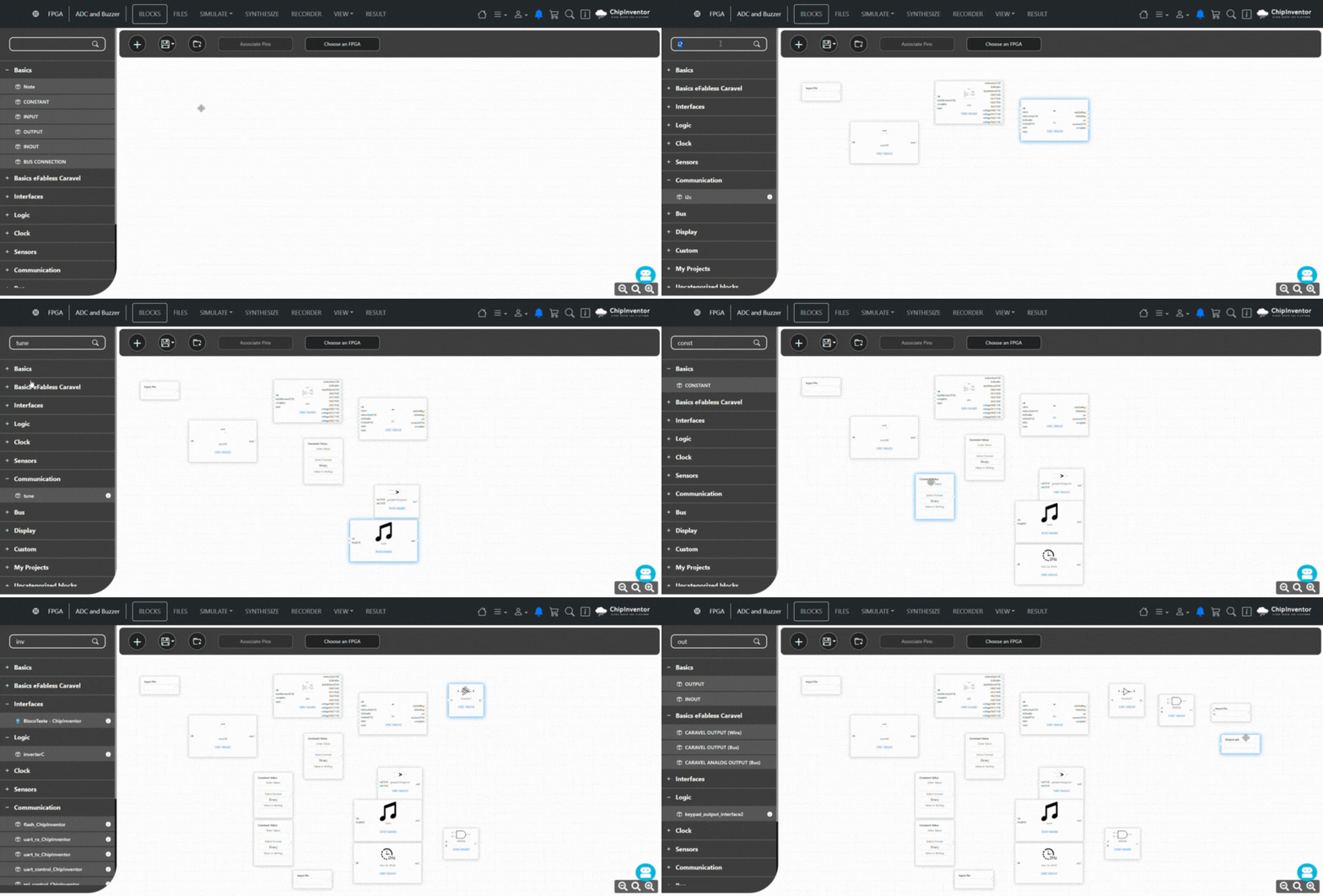
Understanding the Project and the Blocks Used
The basic diagram of this project consists of reading data from an ADC (Analog-to-Digital Converter) via I2C. Then, based on the value read, we compare it to a threshold. If it exceeds that threshold, a buzzer sound is generated at a predefined frequency, with a periodic on/off pulse.
Below is an overview of the main blocks:
1. startAll
-
-
Releases system operation after a few clock cycles, generating the start signal.
-
Ensures that the other blocks only begin read/write operations after a short delay.
-
2. i2c
-
-
Implements the I2C protocol for communication with the ADC.
-
Contains input/output signals for sdaIn, sdaOutReg, and scl, as well as control signals (instruction, i2cEnable, etc.).
-
3. adc
-
-
Internally interfaces with the i2c block to configure and read the ADC value.
-
Sends commands to the ADC (via I2C) and receives the converted data, storing it in registers (e.g., Ch0, Ch1, etc.).
-
Typical output: 16-bit digital values representing the measured analog signal (e.g., Ch0, Ch1, Ch2, Ch3).
-
4. greater
-
-
Compares two 16-bit values, returning 1 if numa is greater than numb.
-
Here, we use it to check whether the ADC value exceeds a certain threshold (e.g., 10000).
-
5. two_hz_clock
-
-
Generates a 2 Hz signal (or a frequency defined by a parameter).
-
Used to pulse or “blink” a signal, in this case, creating an on/off effect for the buzzer periodically.
-
6. tune
-
-
Generates a waveform (square wave) at a desired frequency for the buzzer.
-
Receives the global clock and a frequency parameter (freq).
-
7. and3b, AND2b, inverterC
-
-
Logical blocks that assist in enabling or inhibiting combinational signals, controlling whether the buzzer is active at specific times.
-


No Comments